AMT Develops World's First Chip-Level HBM Test Handler
AMT Develops World's First Chip-Level HBM Test Handler
Posted July. 05, 2023 16:16,
Updated July. 05, 2023 16:16
Enhances Productivity by Detecting Defects in Advance
Secures Market Competitiveness with High Precision and High Quality
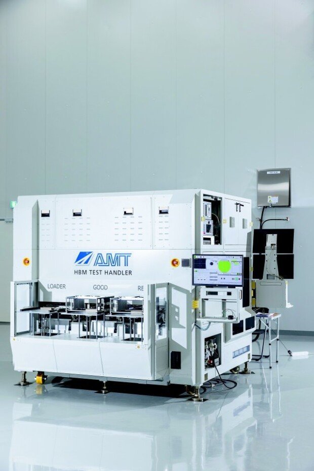
AMT Co., Ltd., a South Korean semiconductor equipment company headquartered in Asan, Chungcheongnam-do, has surprised the industry by announcing a recent success in developing the world's first fine-pitch HBM IC inspection equipment.
The manufacturing of semiconductors involves a sequence of "8 major processes," with the wafer-level process being the foundational step. A circular plate, typically measuring 30 cm in diameter, serves as the wafer, onto which a fine circuit with a thickness of 5 nm (nanometers, where 1 nanometer is equivalent to 1 billionth of a meter) is meticulously etched. Following this, the wafer is divided into individual chips, sometimes referred to as dies. The subsequent stages encompass testing and packaging, commonly known as the back-end processes, which precede the final integration of semiconductors into electronic devices.
AMT's newly developed technology allows for the individual inspection of chips after the assembly and cutting of the HBM (High Bandwidth Memory) device from the wafer stage. The current testing process for high-performance HBM memory utilizes probe cards that employ wafer-scale Micro-Electro-Mechanical Systems (MEMS) technology. HBM, which vertically stacks multiple DRAMs, offers groundbreaking data processing speeds surpassing those of traditional DRAMs, making it a vital component in the technological advancement of the AI era.
Due to the progressive miniaturization of semiconductors, specifically in the context of HBM architecture where the spacing between bumps is extremely tight (referred to as fine pitch spacing), it was previously unfeasible to inspect the individual chips after they were cut from the wafer. Nevertheless, AMT has effectively tackled these obstacles by creating groundbreaking technology and introducing a novel solution that facilitates the expansion of the inspection para.
Previously, the inability to test individual HBM ICs before shipment posed a significant challenge. In the event of defects being discovered by customers after delivery, the entire chipset, including HBM chips integrated with the CPU or GPU, had to be discarded. In such cases, the chip suppliers were responsible for compensating not only for the faulty HBM chips but also for the CPUs or GPUs. However, by implementing the HBM test handler, AMT states that HBM suppliers such as Samsung Electronics, SK Hynix, Micron, and chipset suppliers like TSMC can reduce defect rates, lower costs, improve productivity, and gain a competitive advantage by delivering high-precision, high-quality products. This new technology is expected to significantly expand AMT's market share in the HBM semiconductor inspection equipment industry.
AMT has successfully developed a test handler for next-generation fine pitch ICs used in HBM production testers by SK Hynix and Samsung, as part of a government project. The 64-para test handler, scheduled to be launched by the end of this year, is expected to contribute to significant revenue growth for AMT by leveraging the synergistic effects of this innovative technology.
HBM semiconductor ICs are packaged in wafer form and go through a cutting process. During the inspection, individual HBM ICs need to be arranged at a specific interval, with a dimensional tolerance of within 20μm, to meet the requirements for alignment with probe cards. However, no one in the world including global test handler companies from Japan and Switzerland, was able to implement the technology to achieve device spacing within 20μm. Through two years of internal research and development, AMT was able to bring the precision level to within 10μm.
Founded in 2002, AMT stands out as a team of seasoned experts excelling in semiconductor equipment automation. With a workforce of over 100, with more than half devoted to research and development, AMT truly embraces a technology-intensive approach. The prestigious recognition from the Ministry of Trade, Industry, and Energy in March 2021 further cemented AMT's position as a core strategic technology company in the semiconductor industry. Moreover, AMT's extensive portfolio of over 90 domestic and international patent registrations and applications testifies to its remarkable technological expertise and know-how. With such impressive capabilities, AMT is poised for an exciting future, driving innovation and excellence in the semiconductor equipment sector.
Yoonjung Park ongoh@donga.com