
CIT's New 'CuFlat-PKGCore' Tech Boosts Speed and Efficiency for Next-Gen Semiconductor Packaging.
CIT's New 'CuFlat-PKGCore' Tech Boosts Speed and Efficiency for Next-Gen Semiconductor Packaging.
Posted September. 10, 2025 16:52,
Updated September. 10, 2025 16:55
- CIT has introduced the CuFlat-PKGCore, a key material solution for
semiconductor packaging that enhances speed and efficiency
by consolidating multiple chemical stages into a single deposition process.
- The technology boasts eco-friendly credentials, utilizing 100% recycled copper
scrap and generating no chemical wastewater.
- CIT plans to debut this innovation at CES 2026, aiming for an Innovation Award
and a significant entry into the global semiconductor packaging market.
Materials technology Korean startup ‘CIT’ (Copper Innovation Technologies) has introduced 'CuFlat-PKGCore,' a semiconductor packaging board for AI accelerators, based on its proprietary Atomic Sputtering Epitaxy (ASE) deposition technology.
The CuFlat-PKGCore, a key material for next-generation semiconductor package substrates, is poised to reshape the industry. This enhances design freedom for boards by ensuring a flat and uniform deposition of copper. The innovative process replaces complex chemical procedures with a single deposition step, significantly boosting production speed and efficiency. Furthermore, this manufacturing method minimizes environmental impact by reducing chemical wastewater and carbon emissions. It is expected to cut power and cooling water consumption in data centers by half.
CIT plans to vie for a CES 2026 Innovation Award with the CuFlat-PKGCore and accelerate its entry into the global semiconductor packaging substrate market.
CIT's Breakthrough with ASE Deposition Technology
Founded in 2023, CIT developed the ASE deposition technology, a molecular bonding technique that applies a thin layer of copper onto an insulator. This process creates a single-crystal structure without any separate adhesives, resulting in a uniform surface that remains stable and delamination-free even when exposed to heat.
CIT’s ASE deposition technology has received academic recognition, with features in world-renowned scientific journals such as Nature and Advanced Materials, a leading journal in materials engineering that showcases the latest achievements in advanced materials research and development.
The applications for ASE deposition technology are diverse, spanning high-frequency communication equipment, semiconductor package substrates, displays, and medical and biotech devices. CIT explains that when used to manufacture signal transmission equipment for 5G frequencies of 28GHz and above, the technology significantly improves communication efficiency by reducing signal loss and noise compared to existing materials. Similar benefits are seen in semiconductor package substrates, transparent antennas, and transparent displays.
CIT has already showcased products developed with its ASE technology at major global exhibitions. In January, the company participated in CES 2025 in Las Vegas, and in March, it attended MWC 2025 in Barcelona, presenting its transparent antenna, 'Dolphin,' and a transparent display. According to CIT, the Dolphin antenna covers a broader 20GHz frequency range than existing transparent antennas and is 1,000 times thinner than conventional automotive antenna circuits while boasting a 20% improvement in signal reception performance. These innovations earned the company a CES 2025 Innovation Award.
Last August, CIT was selected as one of the Top 30 International Companies at InnoEX 2025 in Vietnam. Hosted by the Vietnamese Ministry of Science and Technology, InnoEX is the country's largest exhibition, fostering collaboration and growth opportunities within the Asian corporate community.
CIT is also actively building global partnerships. This year, the company is conducting product supply tests with Japan’s AGC (for glass substrates and transparent antennas) and a U.S. semiconductor equipment company. Furthermore, it is jointly developing an AI accelerator substrate with a major South Korean conglomerate, preparing for a joint entry into the global market. Through these collaborations, CIT is expanding the applications of its ultra-flat and ultra-thin technology based on the ASE method.
CuFlat-PKGCore: A Copper-Deposited Glass Substrate for Semiconductor Packaging
CIT's CuFlat-PKGCore technology enhances design freedom by arranging copper atoms into a flat, uniform layer on any type of glass substrate. It streamlines production by replacing a complex, multi-step chemical process with a single deposition process, thereby increasing both speed and efficiency.
The CuFlat-PKGCore achieves a copper surface roughness of less than 3nm on semiconductor packaging glass substrates. This is 200 times smoother than the highest-grade copper foil (HVLP4) currently used in boards for AI accelerator packaging. According to CIT, this remarkable smoothness allows semiconductor packaging engineers to implement their design intentions with perfect fidelity.
The technology is compatible with various glass substrates, including borosilicate and alkali-free types, and can be applied to core and interposer boards. Moreover, unlike conventional copper that oxidizes at 100°C, the CuFlat-PKGCore maintains stability up to 250°C, ensuring no performance degradation in high-temperature environments.
The manufacturing process has also been simplified. Traditional semiconductor package boards for AI accelerators require 3-4 complex chemical stages, including seed layer deposition, electrolytic plating, and chemical-mechanical polishing (CMP). The CuFlat-PKGCore consolidates these into a single deposition process, boosting production efficiency and speed.
The CuFlat-PKGCore also boasts strong eco-friendly credentials. Its manufacturing process generates no chemical wastewater, and it utilizes 100% recycled copper scrap, reducing carbon emissions by over 95%. Energy consumption during production is also minimized. Since the CuFlat-PKGCore operates without performance loss even at 20°C, its application in data-centers could lead to significant savings in power and cooling costs.
CIT plans to debut the CuFlat-PKGCore at CES 2026 in January, where it will also compete for an Innovation Award. Following its 2025 Innovation Award for the Dolphin antenna and transparent display, the company is aiming for a second consecutive win. This will serve as a launchpad for its full-scale entry into the global semiconductor packaging materials market.
"The CuFlat-PKGCore is a key material solution that will accelerate a paradigm shift in the global semiconductor packaging market," said Seung Jung, CEO of CIT. "We plan to simultaneously pursue domestic and export markets, targeting global IT companies in the AI data center, cloud services, and high-performance GPU semiconductor sectors."
By Man-hyuk Han (mh@itdonga.com)
semiconductor packaging that enhances speed and efficiency
by consolidating multiple chemical stages into a single deposition process.
- The technology boasts eco-friendly credentials, utilizing 100% recycled copper
scrap and generating no chemical wastewater.
- CIT plans to debut this innovation at CES 2026, aiming for an Innovation Award
and a significant entry into the global semiconductor packaging market.
Materials technology Korean startup ‘CIT’ (Copper Innovation Technologies) has introduced 'CuFlat-PKGCore,' a semiconductor packaging board for AI accelerators, based on its proprietary Atomic Sputtering Epitaxy (ASE) deposition technology.
The CuFlat-PKGCore, a key material for next-generation semiconductor package substrates, is poised to reshape the industry. This enhances design freedom for boards by ensuring a flat and uniform deposition of copper. The innovative process replaces complex chemical procedures with a single deposition step, significantly boosting production speed and efficiency. Furthermore, this manufacturing method minimizes environmental impact by reducing chemical wastewater and carbon emissions. It is expected to cut power and cooling water consumption in data centers by half.
CIT plans to vie for a CES 2026 Innovation Award with the CuFlat-PKGCore and accelerate its entry into the global semiconductor packaging substrate market.
CIT’s ASE deposition technology, which bonds copper and an insulator into a single-crystal structure / source=CIT
CIT's Breakthrough with ASE Deposition Technology
Founded in 2023, CIT developed the ASE deposition technology, a molecular bonding technique that applies a thin layer of copper onto an insulator. This process creates a single-crystal structure without any separate adhesives, resulting in a uniform surface that remains stable and delamination-free even when exposed to heat.
CIT’s ASE deposition technology has received academic recognition, with features in world-renowned scientific journals such as Nature and Advanced Materials, a leading journal in materials engineering that showcases the latest achievements in advanced materials research and development.
The applications for ASE deposition technology are diverse, spanning high-frequency communication equipment, semiconductor package substrates, displays, and medical and biotech devices. CIT explains that when used to manufacture signal transmission equipment for 5G frequencies of 28GHz and above, the technology significantly improves communication efficiency by reducing signal loss and noise compared to existing materials. Similar benefits are seen in semiconductor package substrates, transparent antennas, and transparent displays.
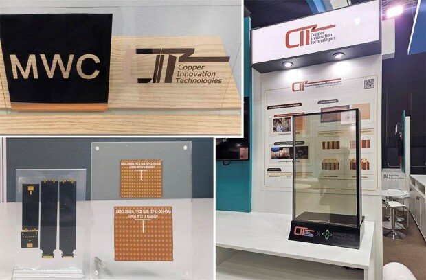
Glass substrate, 5G antenna FPCB, and transparent antenna showcased at MWC 2025 / source=CIT
CIT has already showcased products developed with its ASE technology at major global exhibitions. In January, the company participated in CES 2025 in Las Vegas, and in March, it attended MWC 2025 in Barcelona, presenting its transparent antenna, 'Dolphin,' and a transparent display. According to CIT, the Dolphin antenna covers a broader 20GHz frequency range than existing transparent antennas and is 1,000 times thinner than conventional automotive antenna circuits while boasting a 20% improvement in signal reception performance. These innovations earned the company a CES 2025 Innovation Award.
Last August, CIT was selected as one of the Top 30 International Companies at InnoEX 2025 in Vietnam. Hosted by the Vietnamese Ministry of Science and Technology, InnoEX is the country's largest exhibition, fostering collaboration and growth opportunities within the Asian corporate community.
CIT is also actively building global partnerships. This year, the company is conducting product supply tests with Japan’s AGC (for glass substrates and transparent antennas) and a U.S. semiconductor equipment company. Furthermore, it is jointly developing an AI accelerator substrate with a major South Korean conglomerate, preparing for a joint entry into the global market. Through these collaborations, CIT is expanding the applications of its ultra-flat and ultra-thin technology based on the ASE method.
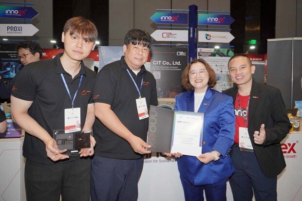
CIT was named a Top 30 International Company at InnoEX 2025 in Vietnam / source=CIT
CuFlat-PKGCore: A Copper-Deposited Glass Substrate for Semiconductor Packaging
CIT's CuFlat-PKGCore technology enhances design freedom by arranging copper atoms into a flat, uniform layer on any type of glass substrate. It streamlines production by replacing a complex, multi-step chemical process with a single deposition process, thereby increasing both speed and efficiency.
The CuFlat-PKGCore achieves a copper surface roughness of less than 3nm on semiconductor packaging glass substrates. This is 200 times smoother than the highest-grade copper foil (HVLP4) currently used in boards for AI accelerator packaging. According to CIT, this remarkable smoothness allows semiconductor packaging engineers to implement their design intentions with perfect fidelity.
The technology is compatible with various glass substrates, including borosilicate and alkali-free types, and can be applied to core and interposer boards. Moreover, unlike conventional copper that oxidizes at 100°C, the CuFlat-PKGCore maintains stability up to 250°C, ensuring no performance degradation in high-temperature environments.
The manufacturing process has also been simplified. Traditional semiconductor package boards for AI accelerators require 3-4 complex chemical stages, including seed layer deposition, electrolytic plating, and chemical-mechanical polishing (CMP). The CuFlat-PKGCore consolidates these into a single deposition process, boosting production efficiency and speed.
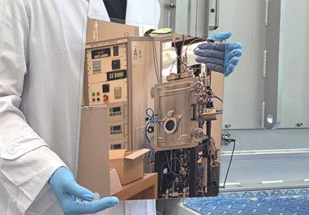
CIT’s CuFlat-PKGCore / source=CIT
The CuFlat-PKGCore also boasts strong eco-friendly credentials. Its manufacturing process generates no chemical wastewater, and it utilizes 100% recycled copper scrap, reducing carbon emissions by over 95%. Energy consumption during production is also minimized. Since the CuFlat-PKGCore operates without performance loss even at 20°C, its application in data-centers could lead to significant savings in power and cooling costs.
CIT plans to debut the CuFlat-PKGCore at CES 2026 in January, where it will also compete for an Innovation Award. Following its 2025 Innovation Award for the Dolphin antenna and transparent display, the company is aiming for a second consecutive win. This will serve as a launchpad for its full-scale entry into the global semiconductor packaging materials market.
"The CuFlat-PKGCore is a key material solution that will accelerate a paradigm shift in the global semiconductor packaging market," said Seung Jung, CEO of CIT. "We plan to simultaneously pursue domestic and export markets, targeting global IT companies in the AI data center, cloud services, and high-performance GPU semiconductor sectors."
By Man-hyuk Han (mh@itdonga.com)


![[단독]김관영 지사, 무소속 출마 결심…6일 출마선언 예정](https://dimg.donga.com/c/138/175/90/1/wps/NEWS/IMAGE/2026/05/03/133854339.1.jpg)
