
Semiconductor makers are in survival game for two nm process
Semiconductor makers are in survival game for two nm process
Posted June. 29, 2023 07:58,
Updated June. 29, 2023 07:58

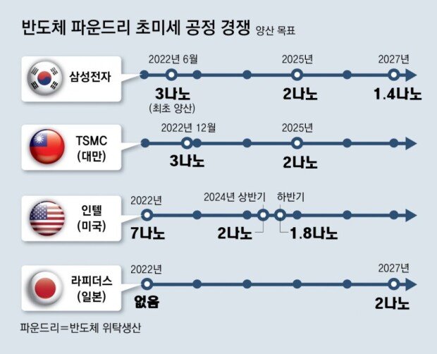
The global foundry market is becoming highly competitive for taking the lead in the two nm process. Almost all semiconductor powerhouses, including South Korea, Taiwan, the United States, and Japan have already rolled up their sleeves to manufacture cutting-edge semiconductors, one of the most essential components for artificial intelligence and autonomous driving.
Samsung Electronics detailed a plan to mass-produce the two nm process at Samsung Foundry Forum 2023 held in Silicon Valley in the United States on Tuesday (local time). With more than 700 foundry clients and partners present, it announced that the company will mass-produce the two nm process for mobile devices, HPCs, and automobiles by 2025, 2026, and 2027, respectively. "The state-of-art two nm process will outcompete the three nm process by 12 percent and 25 percent in performance and power efficiency, respectively, and get smaller than the latter by 5 percent,” it anticipated.
The unit of a nanometer is used in the foundry process to describe the minimum processing linewidth of semiconductors. A narrower linewidth translates into more chips being manufactured on the same size wafer. As it can lead to greater productivity and better performance, foundry companies are vying to realize a hyperfine process. With Samsung and Taiwan's TSMC having made it to the three nm process, the next big thing is the two nm process.
Samsung first released detailed roadmaps for each two nm process product line on Tuesday. "It does not simply mean a mass production goal but implies that the manufacturer already has secured a list of clients for each sector,” said an insider of the semiconductor industry, adding, "It shows how it is confident in front of the competition and the rest of the market.”
Do-Young Kwak now@donga.com

![[단독]전국서 투표용지 4726장 모자랐다…100장 넘게 부족한 17곳 모두 서울](https://dimg.donga.com/c/138/175/90/1/wps/NEWS/IMAGE/2026/06/08/134068891.1.jpg)


![고기 안주랑 먹어야 살 덜 찐다? ‘단백질 미끼’의 함정[바디플랜]](https://dimg.donga.com/c/138/175/90/1/wps/NEWS/IMAGE/2026/06/08/134070571.3.jpg)
