
SK Hynix develops 238-layer NAND flash chip
SK Hynix develops 238-layer NAND flash chip
Posted August. 04, 2022 07:46,
Updated August. 04, 2022 07:46
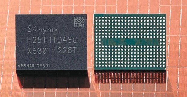
SK Hynix has successfully developed its most advanced 238-layer NAND flash (photo), which is the most layered among the existing NAND flash memory chips. Before SK Hynix, U.S.-based Micron Technology’s chips were the most layered with 232 layers.
On Tuesday (local time), SK Hynix unveiled its new 238-layer 512 Gb triple level cell (TLC) 4D NAND flash product at the world largest NAND flash conference of “Flash Memory Summit 2022” in Santa Clara, California, the U.S. SK Hynix announced that it shipped samples of the chips to client companies and plans to make mass production in the first half of next year.
The latest achievement follows the development of the 176-layer NAND production in December 2020 in one year and seven months. The chip is most layers but also the smallest in the world, which is noteworthy. “SK Hynix gained global top-tier competitiveness in cost, performance, and quality perspective by introducing the 238-layer product leveraging the 4D NAND technologies,” Choi Jeong-dal, head of NAND development at SK Hynix, said in the summit. “We will continue innovations to find breakthroughs in technological limits.”
SK Hynix explains that with this new 238-layer product, overall productivity has increased by 34 percent compared with the former 176-layer NAND. The data transfer speed is 2.4Gb per second, a 50 percent increase from the previous generation. The volume of the energy consumed for data reading has decreased by 21 percent.
The 238-layer products will be first adopted for client SSDs, which are used as PC storage devices, before being provided for smartphones and high-capacity SSDs for servers later. The company will also introduce 238-layer products in 1 Terabit (Tb) next year, with density doubled compared to the current 512Gb product.
Do-Young Kwak now@donga.com


