Samsung chief Lee Jae-yong visits semiconductor R&D center
Samsung chief Lee Jae-yong visits semiconductor R&D center
Posted January. 03, 2020 07:54,
Updated January. 03, 2020 07:54
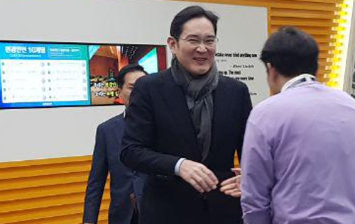
“Our past performance doesn't guarantee success in the future,” said Samsung Electronics Vice Chairman Lee Jae-yong during his visit to a next-generation semiconductor R&D center on Thursday. “History is not what we should wait for – it is what should be made,” he added.
As this was the vice chairman’s first visit to any Samsung Electronics site of the new year, industry experts say it re-emphasizes Samsung’s vision to become a leading player in the system chip sector, which was put forward publicly by the electronics giant last year.
Lee attended a New Year’s celebration held at the international meeting room of the Korea Chamber of Commerce and Industry (KCCI) in Jung-gu, Seoul on Thursday morning and headed straight to the company's chip R&D center in Hwaseong, Gyeonggi Province. He was briefed about the 3-nanometer processing technology, which was first developed by Samsung Electronics in the world, and discussed next-generation semiconductor strategy with senior executives of Samsung’s Device Solutions (DS) Division.
"We must get rid of wrong thoughts and customs and move forward to explore a new future,” said the vice chairman. “We also must remember that growing and sharing with our neighbors and society is our mission and a path to become a company that lasts 100 years and more.”
The New Year’s celebration by Samsung Electronic was presided by Vice Chairman Kim Ki-nam at 9 a.m. on Thursday without Vice Chairman Lee, but Lee’s messages on the chip R&D site are thought to be his New Year’s address. His key message is to realize Samsung’s vision to become the No. 1 player in the system chip sector with technology innovations despite the growing uncertainties, both internally and externally, and fulfill the company’s social responsibilities.
Hyoun-Soo Kim kimhs@donga.com